 SingaporeSG
 ChinaCN
 MalaysiaMY
 IndonesiaID
 MyanmarMM
Material Science & Nanotechnology
- Home
- Products
- Material Science & Nanotechnology
- Material Characterisation
- Hybridized SEM – Spectroscopic Platform (FA CL SEM)
- Allalin - Hybridized SEM - Spectroscopic Platform
Hybridized SEM – Spectroscopic Platform (FA CL SEM)

Allalin - Hybridized SEM - Spectroscopic Platform
Overview
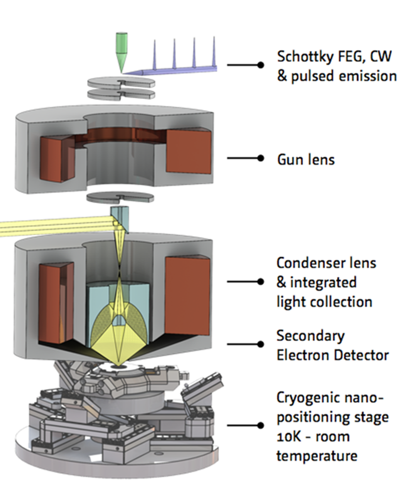
The Allalin is a nanometer resolution spectroscopy instrument, based on a unique and patented system including an optical collection objective integrated within the SEM column.
One platform, multiple possibilities of measurements
This platform offers a very large range of spectroscopic analysis thanks to its multiple sources (electronic, laser in continuous or pulsed mode) and many types of detectors (PMT, CCD/Streak cameras, TCSPC/ADP… detectors, Raman…). In addition, the system can be equipped with various options such as : EBIC system, nanoprobes, HV transfer unit and can welcome small samples from few µm size to wafers up to 6 inches.
The spectroscopic analyses can be conducted at any temperature from RT down to 10K thanks to an integrated Helium cryostat and copper braid coupling ensuring high stability and very low drift.
Features
The base system is a SEM – spectroscopic platform on which multiple options can be adapted:

Sources
- Continuous/pulsed electronic source
- Continuous/pulsed laser
Spectrometers
- up to 2 spectrometers on the platform
Detectors
Continuous detectors
- PMT
- UV-Visible (EM-)CCD camera (from 180nm to 1050nm)
- InGaAs detector (from 900 to 2200nm)
Time-resolved detectors
- Streak camera
- TCSPC detector
Stages
- Nano-positioning stage (cryo-compatible)
- 3’/6’ wafer stage
Options
- Nanoprobes (up to 4 probes)
- Raman line
- EBIC/EBAC
Applications
- Electronics & optoelectronics (GaN, InP, SiC…)
- Photovoltaic cells (GaAs, CdTe, Perovskites…)
- Light emitting diodes (MicroLEDs)
- 2D materials (Graphene, BN, WS2…)
- Noble metals (plasmonic)
- Nano-micro particles
- Nano-micro wires/rods
- Photonic crystals
- Quantum wells & quantum dots
- Minerals, glasses, ceramics and gemstones
- Inorganic coatings
- Polymers layers
- Organic materials
- Biological samples, cells, vesicles
- …
| Features | Kindly refer to the |


Author: K. Loeto, G. Kusch, P-M. Coulon, SM. Fairclough, E. Le Boulbar, I. Girgel, PA. Shields and RA. Oliver
Publication: Nano Express 2 (2021) 014005
Core-shell nanorod based light-emitting diodes (LEDs) with their exposed non-polar surfaces have the potential to overcome the limitations of planar LEDs by circumventing the quantum confined stark effect. In this experiment, InGaN/GaN core-shell nanorods were fabricated by a combination of top-down etching and bottom-up regrowth using metal-organic vapour phase epitaxy. When viewing the nanorods along their long axis, monochromatic cathodoluminescence maps taken at the GaN near-band-edge emission energy (3.39 eV) reveal a ring-like region of lower emission intensity. The diameter of this ring is found to be 530 (±20)nm corresponding to the ~510 nm diameter nickel etch masks used to produce the initial GaN nanopillars. Thus, the dark ring corresponds to the regrowth interface. To understand the origin of the ring, scanning transmission electron microscopy (STEM) and cathodoluminescence (CL) hyperspectral mapping at 10K were performed. STEM imaging reveals the absence of extended defects in the nanorods and indeed near the regrowth interface. Monochromatic CL maps recorded at 10K show that the ring remains dark for monochromatic maps taken at the GaN near-band-edge emission energy (3.47 eV) but is bright when considering the donor-acceptor pair emission energy (3.27 eV). This peculiar anticorrelation indicates that the dark ring originates from an agglomeration of point defects associated with donor-acceptor pair emission. The point defects are incorporated and buried at the GaN regrowth interface from the chemical and/or physical damage induced by etching and lower the radiative recombination rate; limiting the radiative efficiency close to the regrowth interface.
Author: Thomas Bidaud, John Moseley, Mahisha Amarasinghe, Mowafak Al-Jassim, Wyatt K. Metzger, and Stephane Collin
Publication: Phys. Rev. Materials 5, 064601
Postdeposition CdCl2 treatment of polycrystalline CdTe is known to increase the photovoltaic device efficiency. However, the precise chemical, structural, and electronic changes that underpin this improvement are still debated. In this study, spectroscopic photoemission electron microscopy was used to spatially map the vacuum level and ionization energy of CdTe films, enabling the identification of electronic structure variations between grains and grain boundaries (GBs). In vacuo preparation and inert transfer of oxide-free CdTe surfaces isolated the separate effects of CdCl2 treatment and ambient oxygen exposure. Qualitatively, grain boundaries displayed lower work function and downward band bending relative to grain interiors, but only after air exposure of CdCl2-treated CdTe. Analysis of numerous space charge regions at grain boundaries showed an average depletion width of 290 nm and an average band bending magnitude of 70 meV, corresponding to a GB trap density of 1011 cm–2 and a net carrier density of 1015 cm–3. These results suggest that both CdCl2 treatment and oxygen exposure may be independently tuned to enhance the CdTe photovoltaic performance by engineering the interface and bulk electronic structure.
Author: Orri, J. F., Tennyson, E. M., Kusch, G., Divitini, G., Macpherson, S., Oliver, R., Ducati, C., Stranks, S.
Publication: Nano Express (2021)
The use of pulsed mode scanning electron microscopy cathodoluminescence (CL) for both hyperspectral mapping and time-resolved measurements is found to be useful for the study of hybrid perovskite films, a class of ionic semiconductors that have been shown to be beam sensitive. A range of acquisition parameters is analysed, including beam current and beam mode (either continuous or pulsed operation), and their effect on the CL emission is discussed. Under optimized acquisition conditions, using a pulsed electron beam, the heterogeneity of the emission properties of hybrid perovskite films can be resolved via the acquisition of CL hyperspectral maps. These optimized parameters also enable the acquisition of time-resolved CL of polycrystalline films, showing significantly shorter lived charge carriers dynamics compared to the photoluminescence analogue, hinting at additional electron beam-specimen interactions to be further investigated. This work represents a promising step to investigate hybrid perovskite semiconductors at the nanoscale with CL.
Author: R. Ron, M.S. Zielinski, A.Salomon
Publication: Nano Lett. 2020, 20, 11, 8205–8211
Nanoporous metallic networks are endowed with the distinctive optical properties of strong field enhancement and spatial localization, raising the necessity to map the optical eigenmodes with high spatial resolution. In this work, we used cathodoluminescence (CL) to map the local electric fields of a three-dimensional (3D) silver network made of nanosized ligaments and holes over a broad spectral range. A multitude of neighboring hotspots at different frequencies and intensities are observed at subwavelength distances over the network. In contrast to well-defined plasmonic structures, the hotspots do not necessarily correlate with the network morphology, emphasizing the complexity and energy dissipation through the network. In addition, we show that the inherent connectivity of the networked structure plays a key optical role because a ligament with a single connected linker shows localized modes whereas an octopus-like ligament with multiple connections permits energy propagation through the network.
Author: Marco Negri, Luca Francaviglia, Dumitru Dumcenco, Matteo Bosi, Daniel Kaplan, Venkataraman Swaminathan, Giancarlo Salviati, Andras Kis, Filippo Fabbri, Anna Fontcuberta i Morral
Publication: Nano Lett. 2020, 20, 1, 567-576
Two-dimensional semiconductors, in particular transition metal dichalcogenides and related heterostructures, have gained increasing interest as they constitute potential new building blocks for the next generation of electronic and optoelectronic applications. In this work, we develop a novel nondestructive and noncontact technique for mapping the absorption properties of 2D materials, by taking advantage of the underlying substrate cathodoluminescence emission. We map the quantitative absorption of MoS2 and MoSe2 monolayers, obtained on sapphire and oxidized silicon, with nanoscale resolution. We extend our technique to the characterization of the absorption properties of MoS2/MoSe2 van der Waals heterostructures. We demonstrate that interlayer excitonic phenomena enhance the absorption in the UV range. Our technique also highlights the presence of defects such as grain boundaries and ad-layers. We provide measurements on the absorption of grain boundaries in monolayer MoS2 at different merging angles. We observe a higher absorption yield of randomly oriented monolayers with respect to 60° rotated monolayers. This work opens up a new possibility for characterizing the functional properties two-dimensional semiconductors at the nanoscale.
Author: KUSCH, Gunnar, COMISH, Ella J., LOETO, Kagiso, et al.
Publication: Nanoscale, 2022, vol. 14, no 2, p. 402-409.
Time-resolved cathodoluminescence offers new possibilities for the study of semiconductor nanostructures – including defects. The versatile combination of time, spatial, and spectral resolution of the technique can provide new insights into the physics of carrier recombination at the nanoscale. Here, we used power-dependent cathodoluminescence and temperature-dependent time-resolved cathodoluminescence to study the carrier dynamics at trench defects in InGaN quantum wells – a defect commonly found in III-nitride structures. The measurements show that the emission properties of trench defects closely relate to the depth of the related basal plane stacking fault within the quantum well stack. The study of the variation of carrier decay time with detection energy across the emission spectrum provides strong evidence supporting the hypothesis that strain relaxation of the quantum wells enclosed within the trench promotes efficient radiative recombination even in the presence of an increased indium content. This result shines light on previously reported peculiar emission properties of the defect, and illustrates the use of cathodoluminescence as a powerful adaptable tool for the study of defects in semiconductors.
Author: M. Fouchier, N. Rochat, E. Pargon, J. P. Landesman
Publication: Rev. Sci. Instrum. 90, 043701 (2019)
Strain can alter the properties of semiconductor materials. The selection of a strain measurement technique is a trade-off between sensitivity, resolution, and field of view, among other factors. We introduce a new technique based on the degree of polarization of cathodoluminescence (CL), which has excellent sensitivity (10−5), an intermediate resolution (about 100 nm), and an adjustable field of view. The strain information provided is complementary to that obtained by CL spectroscopy. Feasibility studies are presented. The experimental setup and the data treatment procedure are described in detail. Current limitations are highlighted. The technique is tested on the cross section of bulk indium phosphide samples strained by a patterned hard mask.